"...solution is to use silicon germanium in place of elemental silicon for the semiconductor layer. Silicon germanium has a lower bandgap than elemental silicon, such that it is better for the absorption of infrared radiation. However, silicon germanium has poor compatibility with CMOS processes for the logic devices due to increased leakage current. As such, manufacturing the logic devices on silicon germanium introduces difficulties and adds cost to the manufacture of the CMOS image sensors.
The present application is directed to a CMOS image sensor with elemental silicon and silicon germanium for long-wavelength pixel sensors. In some embodiments, an elemental silicon layer abuts a silicon germanium layer. A photodetector is at least partially buried in the silicon germanium layer and a transistor is arranged on a surface of the elemental silicon layer with a source/drain region electrically coupled to the photodetector. By arranging the photodetector in the silicon germanium layer, the photodetector advantageously has good sensitivity to and absorption of long-wavelength radiation, such as, for example, infrared radiation. Further, by arranging the transistor on the elemental silicon layer, conventional CMOS processes may advantageously be used when forming the transistor."
"...the semiconductor stack 102 comprises a silicon layer 104 and a silicon germanium layer 106. In some embodiments, the silicon germanium layer 106 partially covers an upper surface 108 of the silicon layer 104, and/or is buried in the upper surface 108 of the silicon layer 104. In other embodiments, the silicon germanium layer 106 is partially or fully covered by the silicon layer 104. The silicon and silicon germanium layers 104, 106 may correspond to epitaxial layers and/or regions of a semiconductor substrate, and the silicon layer 104 may be, for example, elemental silicon."


Another TSMC patent application US20170141148 "Infrared image sensor component and manufacturing method thereof" by Chien-ying Wu, Li-hsin Chu, Chung-chuan Tseng, Chia-wei Liu is somewhat similar, but integrates InGaAs sensing layer in a CMOS process flow:
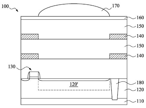
"The infrared sensor component includes a substrate [110], a III-V compound layer [120] disposed on the substrate as an active pixel region, and a plurality of transistors formed on the III-V compound layer. The III-V compound layer is made of III-V groups materials, which have wide infrared wavelength coverage, large absorption coefficient in the infrared region, and high carrier mobility. Therefore, the performance of the infrared image sensor component can be improved accordingly."
Anything new?
ReplyDeleteNo.
DeleteResurection of Nobel Peak ?
ReplyDeleteWhat's the difference between noblepeak?
ReplyDelete